
Chip Pins
An online reference from Dig Dug reveals the following.
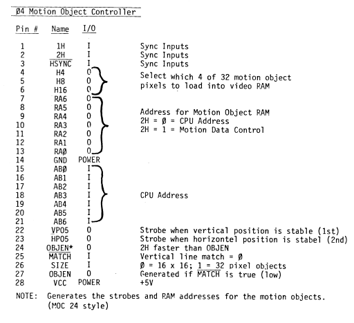
The following restates that table with connection information in Pole Position.
| Pin | Name | IO | Signal in Pole Position |
|---|---|---|---|
| 1 | 1H | I | HPOS0(1H) |
| 2 | 2H | I | HPOS1(2H) |
| 3 | /HSYNC | I | /HSYNC |
| 4 | H4 | O | H4* |
| 5 | H8 | O | H8* |
| 6 | H16 | O | H16* |
| 7 | RA6 | O | RAM A6 |
| 8 | RA5 | O | RAM A5 |
| 9 | RA4 | O | RAM A4 |
| 10 | RA3 | O | RAM A3 |
| 11 | RA2 | O | RAM A2 |
| 12 | RA1 | O | RAM A1 |
| 13 | RA0 | O | RAM A0 |
| 14 | GND | P | GND |
| 15 | AB0 | I | AB1 |
| 16 | AB1 | I | AB2 |
| 17 | AB2 | I | AB3 |
| 18 | AB3 | I | AB4 |
| 19 | AB4 | I | AB5 |
| 20 | AB5 | I | AB6 |
| 21 | AB6 | I | AB7 |
| 22 | VPOS | O | /VSET |
| 23 | HPOS | O | /HSET |
| 24 | OBJEN* | O | LDEN |
| 25 | /MATCH | I | /MATCH |
| 26 | SIZE | I | SIZE7 |
| 27 | OBJEN | O | NC |
| 28 | VCC | P | +5V |
Notably, the OBJEN signal is not used in Pole Position.
Theory of Operation
Context
It seems that Pole Position assembles a line buffer of motion object (sprite) pixels, in a double-buffer arrangement. That is, while the current raster line pixels are ouput to the CRT, the buffer for the next raster line is assembled. This provides a budget of 384 pixel clocks to assemble each line.
Horizontal Position
We know from previous analysis of the Namco 07xx, that the rising edge of /HSYNC aligns with horizontal position HPOS[8:0]=336. We speculate therefore the Namco 04xx maintains an internal sprite index counter that is reset with /HSYNC.
The fastest clock available to Namco 04xx is the HPOS0(1H) signal which toggles at half the PIXCLK rate.
We also know from previous analysis of PAL-1, that the Z8002 CPUs are forced into wait-states when accessing the external bus while HPOS1(2H) is high. This is consistent with the text description, indicating that when input 2H is high, the chip performs Motion Data Control.
Motion Object RAM
In Pole Position, the Motion Object RAM consists of eight 2114 chips, each providing 1k x 4-bits of storage. These are grouped as:
- two chips form a 1k x 8-bit area including motion SIZE buffers, accessed on the MSB of the external bus,
- two chips form a 1k x 8-bit area including motion DATA buffers, accessed on the LSB of the external bus, and
- four chips form a 1k x 16-bit area including motion POSI buffers.
Only the bus masters, e.g. the Z8002 CPUs, can assert the /WE signal and cause the Motion Object RAMs to be written (the /WE signal itself is generated on schematic sheet 12A). Otherwise, these RAMs are driving their data outputs with adressed content.
It's evident that when HPOS1(2H) is low, the external bus master is in control of the RAM address, and therefore the Namco 04xx simply passes the input AB[6:0] through to the output RA[6:0]. Otherwise, when HPOS1(2H) is high, the Namco 04xx generates RA[6:0] from its internal state.
We note that in Pole Position, the bus AB[10:8] drive the RAM address bits A[9:7] when HPOS1(2H) is low. However, when HPOS1(2H) is high, the top three RAM address bits are all set high. This carves out only the most-significant 128 addresses for motion objects. The remainder of this RAM is only visible by the bus masters, and therefore general-purpose RAM.
Speculating On Internal State
We know that in Pole Position, the Namco 04xx RA[6:0] selects a 32-bit word in Motion Object RAM. That word maps as:
- D[31:24] => SIZE[7:0],
- D[23:16] => DATA[7:0], and
- D[9:0] => POSI[9:0].
We now look at how these slices are consumed for some hints about how the 04xx chip updates its outputs.
/MATCH Generation
On sheet 14A of the Pole Position schematic, we find the Match Circuit. A simplified block diagram appears below.
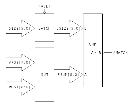
We note that the /MATCH signal asserts when (VPOS[7:0] + POSI[8:0]) >= LSIZE[5:0], where SIZE is left-extended with zeroes. When /VSET asserts, LSIZE is frozen to the current value of SIZE.
A simplified expression for the /MATCH condition is VPOS >= (SIZE - POSI). It follows that POSI values are generally negative.
It seems reasonable to assume the Namco 04xx /VSET output is influenced by the state of the /MATCH input. More on that below.
RAM Layout Implies Line Sweep
It is apparent from the MAME sources that the RAM managed by the Namco 04xx supports 64 sprites. The 128 32-bit words in the RAM are actually 64 consecutive word-pairs, one pair per sprite.
| Word Offset | SIZE[7:0] | DATA[7:0] | POSI[9:0] |
|---|---|---|---|
| 0 | yscale[5:0], big[7] | code[6:0], flipx[7] | sy = 511 - [8:0] |
| 1 | xscale[5:0] | color[5:0] | sx = [9:0] - 60 |
Given the line buffer assembly operation downstream, we speculate that the interal state of the Namco 04xx simply sweeps across all sprite memory after each HSYNC pulse (but only when 2H is high), such that downstream hardware composes a line buffer of sprite pixels.
LDEN, /VSET and /HSET Coordination
Downstream of the RAMs, hardware latches the data word 0 with /VSET, and data word 1 with /HSET. One refinement to our word offsets, which is consistent with the speculations, is that word 0 is vertical information, and word 1 is horizontal. The Namco 04xx advances through sprites until /MATCH is asserted, which indicates that a sprite collides with the current scan line being assembled. Then, /VSET is pulsed to store the first word of the sprite, which corresponds to all vertical information. Then, the next RAM address is selected and /HSET is pulsed to store the second word of the sprite, which corresponds to all horizontal information.
The LDEN drives another custom Namco chip (02xx) which appears responsible for selecting the actual bitmap pixels for output to the raster line buffer.
H4, H8, and H16 Outputs
Downstream circuitry advances through sprite bitmap pixels by using these outputs. These three bits select a 16-bit bitmap ROM word, which contains four contiguous 4-bit pixels. Presumably these outputs only advance when there is a sprite /MATCH. These outputs are likely advanced as the input HPOS[1:0] advances from 11b to 00b.
The Namco 04xx SIZE input is tied to the SIZE7 bit, which is presumable the same value for both vertical and horizontal Motion Object RAM words in a given sprite.
The SIZE input appears to cause the Namco 04xx to operate on either 16-bit or 32-bit sprites. In the former case, it is assumed the H16 output remains zero, and the internal state advances to the next sprite when H4 and H8 are both asserted. In the latter case, the count continues with H16 set, until all three output bits are asserted before advancing.
Summary and Further Work
The Namco 04xx coordinates the access to sprite RAM, for both the CPU R/W activity, and for rasterizing sprite bitmaps to downstream line buffers.
Assuming the internal Namco 04xx sweep has access to half the PIXCLK cycles (due to the 2H access lockout), the chip could sweep through 192 non-matching sprites per scan line. When a sprite matches, two states are required to latch the vertical and horizontal RAM words, and either 4 states (for 16-bit sprites) or 8 states (for 32-bit sprites) are required to stream out the bitmap pixels.
It is therefore not possible to render all 64 sprites on a single raster line: there simply aren't enough clock cycles available. Furthermore, early indices are preferred over latter, since even non-intersecting sprites take states to skip over. It is assumed that Pole Position limits the number of sprites in use to a relatively small number.
Even without verifying the internal operation of the Namco 04xx, we have enough information to further analyze the downstream sprite processing circuitry. We will do this in subsequent articles.